- 您现在的位置:买卖IC网 > Sheet目录1234 > NP1500SCT3G (ON Semiconductor)THYRISTOR TSPD 100A 150V SMB
�� �
�
�NCP1500�
�DETAILED� OPERATING� DESCRIPTION�
�Introduction�
�The� NCP1500� is� a� dual� mode� regulator� intended� for� use�
�in� baseband� supplies� for� portable� equipment.� Its� unique�
�features� provide� power� to� the� baseband� circuitry� while,� at�
�the� same� time� save� valuable� battery� energy.� When� the�
�handset� is� idle,� the� user� can� activate� the� linear� regulator�
�function.� In� this� mode,� the� regulator� provides� a� regulated�
�low� current,� low� noise� output� voltage� keeping� the� baseband�
�circuit� biased.� When� the� handset� is� in� its� normal� operating�
�mode,� the� regulator� synchronizes� to� the� baseband� clock� and�
�turns� into� a� switching� regulator.� This� allows� the� regulator� to�
�provide� efficient� power� to� the� baseband� circuit.�
�Operating� Description�
�Synchronization� Protocol� and� Mode� Selection�
�The� NCP1500� has� a� SYNC� input.� The� device� operates� at�
�a� fixed� switch� frequency� determined� by� the� frequency� of� the�
�synchronization� signal� applied.� The� part� automatically�
�operates� in� PWM� mode� after� synchronization� pulses� are�
�present� for� several� cycles.� The� NCP1500� will� output� 2�
�pulses� when� a� sync� signal� is� present.� The� first� is� a� PWM�
�pulse.� This� pulse� ‘sets’� a� latch� that� initiates� output� switch�
�conduction.� The� width� of� this� pulse� controls� the� minimum�
�on� time� in� PWM� mode.� The� second� signal� is� a� slope�
�compensation� ramp.� A� ramp� signal� is� generated.� This� signal�
�is� summed� with� the� current� information� before� being� fed�
�into� the� PWM� comparator.� The� purpose� of� this� circuit� is� to�
�provide� stable� operation� at� output� switch� duty� cycles� in�
�excess� of� 50%.� The� device� automatically� switches� to� linear�
�mode� when� the� SYNC� signal� is� removed� for� approximately�
�6.0� m� sec� .� It� is� recommended� that� the� sync� signal� be�
�externally� pulled� low� to� enable� the� linear� mode� .� Pulling�
�the� pin� high� or� open� may� cause� portions� of� the� circuit� to�
�remain� active,� increasing� the� total� current� consumption� of�
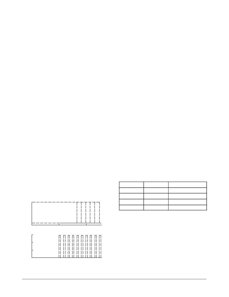
�Figure� 3� shows� the� waveform� when� the� SYNC� signal� is�
�applied.� After� several� cycles,� the� MODE� select� changes� and�
�PWM� operation� is� activated� with� the� internal� clock� signal.�
�Reference/Shutdown�
�The� NCP1500� uses� an� internal� reference,� typically� at�
�0.8� V.� An� external� shutdown� pin� is� provided.� When� this� pin�
�is� pulled� low,� the� reference� and� other� circuitry� are� disabled,�
�placing� the� part� into� a� low� quiescent� current� standby� mode.�
�In� this� mode,� the� pass� device� is� off� and� the� output� voltage�
�will� be� zero.� The� typical� standby� current� is� 0.18� m� A.�
�Error� Amplifier/Output� Voltage� Program�
�A� fully� compensated� error� amplifier� is� provided� inside� the�
�NCP1500.� No� external� circuitry� is� required� to� stabilize� the�
�operation� of� the� NCP1500.� The� error� amplifier� provides� an�
�error� signal� to� both� the� PWM� circuit� and� the� linear� regulator�
�circuit.� The� output� of� the� error� amplifier� is� directly�
�connected� to� the� linear� regulator� control� circuit.� However,�
�the� output� of� the� error� amplifier� is� connected� first� to� a�
�subtraction� circuit� before� going� to� the� input� of� the� PWM�
�comparator.� The� subtraction� circuit� is� activated� only� during�
�an� over� current� condition.� During� this� condition,� a� signal�
�proportional� to� the� amount� of� over� current� is� subtracted� from�
�the� error� amplifier� signal.� This� subtraction� results� in� a� lower�
�signal� applied� to� the� PWM� comparator,� thus� lowering� the�
�output� duty� cycle.�
�The� output� voltage� is� digitally� programmable� up� to� four�
�voltages.� Two� program� pins� are� provided� to� accomplish� this�
�task.� The� program� pins� control� a� mux,� which� switch� a� bank�
�of� resistors.� The� appropriate� resistor� bank� is� switched� to� the�
�error� amplifier� input,� depending� on� the� program� input.� The�
�following� truth� table� can� be� used� to� program� the� output�
�voltage:�
�the� IC.� The� threshold� level� of� the� SYNC� signal� is� typically�
�1.3� V.� The� duty� cycle� of� the� sync� signal� must� be� within� 20�
�to� 80%.�
�CB0�
�0�
�CB1�
�0�
�Output� Voltage�
�1.5�
�V� IN�
�Internal� CLK� Signal�
�0�
�1�
�1�
�1�
�0�
�1�
�1.8�
�1.3�
�1.0�
�Both� program� pins� are� internally� pulled� low.� Thus,� if� the�
�0�
�3.0�
�External� SYNC� Signal�
�input� pins� are� left� open,� the� output� voltage� will� be� 1.5� V.�
�0�
�0�
�TIME� (� m� )�
�10�
�Figure� 3.� Timing� Diagram� of� the� SYNC� Signal�
�http://onsemi.com�
�5�
�发布紧急采购,3分钟左右您将得到回复。
相关PDF资料
NP2600SCMCT3G
IC TSPD SURGE DEVICE 150MA SMB
NP3100SBMCT3G
IC TSPD SURGE PROTECT 80A SMB
NP3500SCT3G
IC THY SURGE PROTECTOR 350V SMB
NPB02DVFN-RC
CONN JUMPER SHORTING 1.27MM GOLD
NPB02SVAN-RC
CONN JUMPER SHORTING 1.27MM GOLD
NPB02SVFN-RC
CONN JUMPER SHORTING 1.27MM GOLD
NPC02SXNN-RC
CONN JUMPER SHORTING .100" GOLD
NPC02SXON-RC
CONN JUMPER SHORTING .100" GOLD
相关代理商/技术参数
NP1500SDMCT3G
制造商:ONSEMI 制造商全称:ON Semiconductor 功能描述:High Current TSPD
NP1500U
制造商:ORION POWER SYSTEMS, INC. 功能描述:UPS; Network Pro 1500 Line Interactive; Rated at 1500 VA and 1300 Watts
NP15P04SLG-E1-AY
功能描述:MOSFET P-CH -40V MP-3ZK/TO-252 RoHS:是 类别:分离式半导体产品 >> FET - 单 系列:- 标准包装:1,000 系列:MESH OVERLAY™ FET 型:MOSFET N 通道,金属氧化物 FET 特点:逻辑电平门 漏极至源极电压(Vdss):200V 电流 - 连续漏极(Id) @ 25° C:18A 开态Rds(最大)@ Id, Vgs @ 25° C:180 毫欧 @ 9A,10V Id 时的 Vgs(th)(最大):4V @ 250µA 闸电荷(Qg) @ Vgs:72nC @ 10V 输入电容 (Ciss) @ Vds:1560pF @ 25V 功率 - 最大:40W 安装类型:通孔 封装/外壳:TO-220-3 整包 供应商设备封装:TO-220FP 包装:管件
NP15P06SLG-E1-AY
功能描述:MOSFET P-CH -60V MP-3ZK/TO-252 RoHS:是 类别:分离式半导体产品 >> FET - 单 系列:- 标准包装:1,000 系列:MESH OVERLAY™ FET 型:MOSFET N 通道,金属氧化物 FET 特点:逻辑电平门 漏极至源极电压(Vdss):200V 电流 - 连续漏极(Id) @ 25° C:18A 开态Rds(最大)@ Id, Vgs @ 25° C:180 毫欧 @ 9A,10V Id 时的 Vgs(th)(最大):4V @ 250µA 闸电荷(Qg) @ Vgs:72nC @ 10V 输入电容 (Ciss) @ Vds:1560pF @ 25V 功率 - 最大:40W 安装类型:通孔 封装/外壳:TO-220-3 整包 供应商设备封装:TO-220FP 包装:管件
NP15P06SLG-E2-AY
制造商:Renesas Electronics Corporation 功能描述:
NP16
制造商:未知厂家 制造商全称:未知厂家 功能描述:16 AMPERE SILICON RECTIFIER
NP1-6
制造商:Dantona Industries 功能描述:ENERSYS NP1-6 6 VOLT SEALED LEAD ACID BATTERY 制造商:YUASA 功能描述:BATTERY 6V 1AH 制造商:Yuasa Battery Inc 功能描述:BATTERY, 6V, 1AH
NP160CR832K12E
制造商:NYLOK 功能描述: